- 您现在的位置:买卖IC网 > Sheet目录1905 > ATMEGA328P-15AZ (Atmel)MCU AVR 32K FLASH 15MHZ 32-TQFP
2010-2012 Microchip Technology Inc.
DS41413C-page 201
PIC12(L)F1822/PIC16(L)F1823
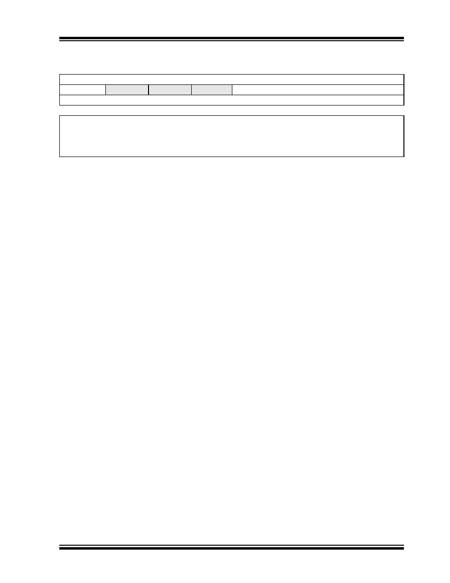
REGISTER 23-2:
MDSRC: MODULATION SOURCE CONTROL REGISTER
R/W-x/u
U-0
R/W-x/u
MDMSODIS
—
—MDMS<3:0>
bit 7
bit 0
Legend:
R = Readable bit
W = Writable bit
U = Unimplemented bit, read as ‘0’
u = Bit is unchanged
x = Bit is unknown
-n/n = Value at POR and BOR/Value at all other Resets
‘1’ = Bit is set
‘0’ = Bit is cleared
bit 7
MDMSODIS:
Modulation Source Output Disable bit
1
= Output signal driving the peripheral output pin (selected by MDMS<3:0>) is disabled
0
= Output signal driving the peripheral output pin (selected by MDMS<3:0>) is enabled
bit 6-4
Unimplemented:
Read as ‘0’
bit 3-0
MDMS<3:0>
Modulation Source Selection bits
1111
= Reserved. No channel connected.
1110
= Reserved. No channel connected.
1101
= Reserved. No channel connected.
1100
= Reserved. No channel connected.
1011
= Reserved. No channel connected.
1010
= EUSART TX output
1001
= Reserved. No channel selected.
1000
= MSSP1 SDO1 output
0111
= Comparator 2 output (PIC16(L)F1823 only. PIC12(L)F1822; Reserved, no channel connected.)
0110
= Comparator 1 output
0101
= Reserved. No channel connected.
0100
= Reserved. No channel connected.
0011
= Reserved. No channel connected.
0010
= CCP1 output (PWM Output mode only)
0001
= MDMIN port pin
0000
= MDBIT bit of MDCON register is modulation source
Note 1:
Narrowed carrier pulse widths or spurs may occur in the signal stream if the carrier is not synchronized.
发布紧急采购,3分钟左右您将得到回复。
相关PDF资料
ATMEGA32L-8PJ
IC MCU AVR 32K 5V 8MHZ 40-DIP
ATMEGA32M1-AUR
IC MPU AVR 32K 20MHZ 32TQFP
ATMEGA48PA-MMNR
MCU AVR 4KB FLASH 20MHZ 28QFN
ATMEGA644P-B15MZ
IC MCU 8BIT 64KB FLASH 32VQFN
ATMEGA644V-10PU
IC AVR MCU FLASH 64K 40DIP
ATMEGA645V-8MI
IC AVR MCU FLASH 64K 1.8V 64QFN
ATMEGA649-16MI
IC AVR MCU FLASH 64K 5V 64QFN
ATMEGA649V-8MI
IC AVR MCU FLASH 64K 1.8V 64QFN
相关代理商/技术参数
ATMEGA328P-15MZ
功能描述:8位微控制器 -MCU 32KB In-system Flash 20MHz 1.8V-5.5V RoHS:否 制造商:Silicon Labs 核心:8051 处理器系列:C8051F39x 数据总线宽度:8 bit 最大时钟频率:50 MHz 程序存储器大小:16 KB 数据 RAM 大小:1 KB 片上 ADC:Yes 工作电源电压:1.8 V to 3.6 V 工作温度范围:- 40 C to + 105 C 封装 / 箱体:QFN-20 安装风格:SMD/SMT
ATMEGA328P-20AU
制造商:Atmel Corporation 功能描述:MCU 8-bit ATmega AVR RISC 32KB Flash 3.3V/5V 32-Pin TQFP
ATMEGA328P20MU
制造商:Atmel Corporation 功能描述:MCU 8-Bit ATmega AVR RISC 32KB Flash 3.3V/5V 32-Pin MLF
ATMEGA328P-AN
功能描述:8位微控制器 -MCU AVR 32K FLSH 2K SRAM 1KB EE-20 MHZ 105C RoHS:否 制造商:Silicon Labs 核心:8051 处理器系列:C8051F39x 数据总线宽度:8 bit 最大时钟频率:50 MHz 程序存储器大小:16 KB 数据 RAM 大小:1 KB 片上 ADC:Yes 工作电源电压:1.8 V to 3.6 V 工作温度范围:- 40 C to + 105 C 封装 / 箱体:QFN-20 安装风格:SMD/SMT
ATMEGA328P-ANR
功能描述:8位微控制器 -MCU AVR 32K FLSH 2K SRAM 1KB EE-20 MHZ 105C
RoHS:否 制造商:Silicon Labs 核心:8051 处理器系列:C8051F39x 数据总线宽度:8 bit 最大时钟频率:50 MHz 程序存储器大小:16 KB 数据 RAM 大小:1 KB 片上 ADC:Yes 工作电源电压:1.8 V to 3.6 V 工作温度范围:- 40 C to + 105 C 封装 / 箱体:QFN-20 安装风格:SMD/SMT
ATMEGA328P-AU
功能描述:8位微控制器 -MCU 32KB In-system Flash 20MHz 1.8V-5.5V
RoHS:否 制造商:Silicon Labs 核心:8051 处理器系列:C8051F39x 数据总线宽度:8 bit 最大时钟频率:50 MHz 程序存储器大小:16 KB 数据 RAM 大小:1 KB 片上 ADC:Yes 工作电源电压:1.8 V to 3.6 V 工作温度范围:- 40 C to + 105 C 封装 / 箱体:QFN-20 安装风格:SMD/SMT
ATMEGA328P-AU SL383
制造商:Atmel Corporation 功能描述:AVR 32K FLASH, 1K EE, 2K SRAM - 20 MHZ, TQFP, IND TEMP GREEN - Tape and Reel
ATMEGA328P-AUR
功能描述:8位微控制器 -MCU AVR 32K FLSH 2K SRAM 1KB EE-20MHz IND
RoHS:否 制造商:Silicon Labs 核心:8051 处理器系列:C8051F39x 数据总线宽度:8 bit 最大时钟频率:50 MHz 程序存储器大小:16 KB 数据 RAM 大小:1 KB 片上 ADC:Yes 工作电源电压:1.8 V to 3.6 V 工作温度范围:- 40 C to + 105 C 封装 / 箱体:QFN-20 安装风格:SMD/SMT